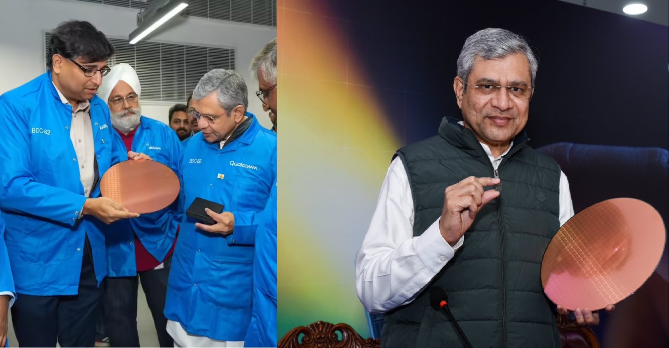
Bengaluru : India has completed the design and tape-out of a 2-nanometer (2nm) semiconductor chip, marking a significant step in the country’s advanced technology capabilities. The development was formally announced by Union Minister for Electronics and Information Technology, Ashwini Vaishnaw, at Qualcomm’s Bengaluru facility, where the work was carried out by Indian engineering teams.
The 2nm node represents the most advanced level of semiconductor design currently achievable, operating at the limits of silicon physics. With this achievement, India joins a small group of regions—including the United States, South Korea, Taiwan, Japan, and parts of Europe—that are capable of developing architectures at this scale. China, by comparison, remains at around the 7-nanometer level due to restrictions on access to Extreme Ultraviolet (EUV) lithography systems required for advanced manufacturing.
Design Milestone at the Frontier of Silicon Technology
The completed tape-out confirms that the full chip design cycle—from product definition and architecture to physical design and validation—was executed in India. Tape-out is the final stage of the design process before fabrication, indicating that the layout is ready to be manufactured at an advanced foundry.
According to technical details shared during the announcement, each die on the 2nm wafer integrates approximately 20 to 30 billion transistors. The design combines high-performance central processing unit (CPU) cores with graphics processing unit (GPU) functionality on a single die. Compared with 3nm technology, 2nm designs typically deliver around 15 percent higher performance and up to 30 percent lower power consumption, improving efficiency for both computing and battery-powered devices.
The architecture is optimized for edge artificial intelligence workloads, enabling on-device AI processing without continuous reliance on cloud infrastructure. Target applications include smartphones, autonomous vehicles, satellites, advanced Wi-Fi routers, data-intensive industrial systems, and defense platforms.
Role of Indian Engineering Centers
The project was executed by Indian engineers working across Qualcomm’s research and development centers in Bengaluru, Chennai, and Hyderabad. These centers collectively represent Qualcomm’s largest engineering base outside the United States. Officials noted that nearly one-fifth of the global semiconductor design workforce is now based in India, reflecting the country’s growing importance in high-end chip design rather than only support and services.
Speaking at the unveiling, Vaishnaw said the achievement demonstrates a shift in India’s role within the global technology ecosystem. He emphasized that India is now participating across the full semiconductor value chain on the design side, rather than being limited to back-end engineering functions.
Strategic and Geopolitical Context
Semiconductors have become a core element of national economic and strategic strength, particularly as artificial intelligence, high-performance computing, and modern defense systems increasingly depend on advanced chips. Manufacturing processes below 5nm require EUV lithography tools produced by ASML, access to which is restricted for certain countries under US-led export controls. While these constraints have limited progress in some regions, India has advanced through a design-first approach that secures intellectual property and system-level expertise, even as domestic fabrication capabilities are still developing.
By completing a 2nm design, India now holds the technical knowledge and design IP required for next-generation hardware platforms. This positions the country to influence future standards and collaborate with leading global foundries for manufacturing, while continuing to expand its production ecosystem.
Semicon India Mission 2.0 and Future Plans
The government has linked the milestone to the transition toward Semicon India Mission 2.0. The first phase of the mission focused on building foundational infrastructure and human capital, including the training of approximately 67,000 engineers in semiconductor-related disciplines over four years. As of now, 315 universities offer specialized semiconductor curricula.
The next phase will prioritize indigenous chip design by supporting Indian startups and product companies, advancing domestic fabrication from current 28nm capabilities toward 7nm and, over time, 2nm, and strengthening the local supply chain by attracting equipment, materials, and specialty gas suppliers. Officials also pointed to ongoing investments of around $70 billion in domestic data center infrastructure, which are expected to increase demand for advanced processors designed in India.
Broader Implications
The successful design and tape-out of a 2nm chip places India firmly within the global group of advanced semiconductor design leaders. While large-scale manufacturing at this node will still depend on international foundries in the near term, the achievement establishes India’s capability at the highest level of chip architecture and system design.
Government and industry officials view the milestone as a foundation for long-term goals to build a self-reliant, globally competitive semiconductor ecosystem by the end of the decade, with India playing a central role in the development of future computing, artificial intelligence, and strategic technologies.
——— End of Article ———