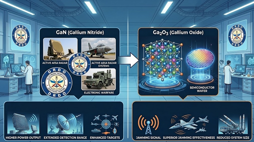
NEW DELHI — March 23, 2026 : India’s Defence Research and Development Organisation (DRDO) has initiated development of Gallium Oxide (Ga₂O₃) semiconductor technology for next-generation radar and electronic warfare (EW) systems, following the successful indigenisation and operational integration of Gallium Nitride (GaN) devices across multiple defense platforms.
The programme is being led by the Solid State Physics Laboratory (SSPL) in Delhi and represents a transition toward ultra-wide bandgap (UWBG) semiconductor materials aimed at supporting future high-power, high-frequency defense electronics.
Gallium Oxide Technology and Core Properties
Gallium Oxide (Ga₂O₃) is classified as a fourth-generation ultra-wide bandgap semiconductor with a bandgap of approximately 4.8–4.9 electron volts (eV), compared with 3.4 eV for GaN and 1.1 eV for silicon.
The material exhibits a critical breakdown electric field of around 8 megavolts per centimetre (MV/cm), more than double that of GaN at 3.3 MV/cm. These properties enable devices based on Ga₂O₃ to operate at higher voltages, deliver greater power density, and support more compact high-frequency radio-frequency (RF) systems.
In practical terms, Ga₂O₃ is intended to enable the development of high-efficiency power amplifiers for Active Electronically Scanned Array (AESA) radars, allowing increased transmission power from smaller antenna modules and improved signal resolution.
Applications in Radar and Electronic Warfare
Ga₂O₃-based devices are expected to support next-generation AESA radar systems with enhanced detection capabilities, particularly against low-observable (stealth) targets. Defense estimates indicate that such systems could potentially detect and track stealth aircraft at ranges between 360 and 600 kilometers, depending on system configuration and integration.
In electronic warfare applications, the material’s high power-handling capability supports wideband jamming, signal intelligence, and electronic countermeasure operations, enabling more effective disruption of adversary radar and communication systems.
The technology is also applicable to space-based systems, including missile warning sensors and radiation-hardened electronics, due to its inherent resistance to high-radiation environments.
Development Work and Institutional Roles
The SSPL is currently focused on establishing indigenous epitaxial growth processes for Ga₂O₃ materials. These processes form the foundation for high-performance electronic and optoelectronic devices, including solar-blind ultraviolet photodetectors capable of detecting missile launches, rocket plumes, and aircraft exhaust signatures without interference from sunlight.
Following material development and optimization, prototype Ga₂O₃ monolithic microwave integrated circuits (MMICs) are planned to be transferred to the Gallium Arsenide Enabling Technology Centre (GAETEC) in Hyderabad for fabrication of RF and microwave components.
DRDO has also initiated collaborative programmes with academic institutions, including the Indian Institute of Technology (IIT) Ropar, focusing on process optimisation and development of thermally stable Ga₂O₃-based devices.
Comparison with GaN-Based Systems
GaN technology currently underpins several modern Indian radar systems, including the Uttam AESA radar, offering improved efficiency and performance over earlier gallium arsenide (GaAs)-based systems.
Key comparative parameters between GaN and Ga₂O₃ include:
-
Bandgap: GaN (3.4 eV) vs Ga₂O₃ (4.8–4.9 eV)
-
Breakdown Field: GaN (3.3 MV/cm) vs Ga₂O₃ (~8 MV/cm)
-
Electron Mobility: GaN (>1,500 cm²/V·s) vs Ga₂O₃ (~150–300 cm²/V·s)
-
Thermal Conductivity: GaN (>200 W/m·K) vs Ga₂O₃ (10–27 W/m·K)
While Ga₂O₃ offers superior voltage handling and power density, it has significantly lower thermal conductivity, which presents a primary engineering challenge.
To address this, DRDO is evaluating advanced thermal management approaches, including integration with silicon carbide (SiC) or diamond substrates, as well as specialized packaging and cooling techniques.
Manufacturing and Material Advantages
Unlike GaN, which relies heavily on complex epitaxial growth processes, Ga₂O₃ can be produced using melt-growth techniques such as Czochralski and edge-defined film-fed growth (EFG) methods. These processes allow for the production of larger wafers at potentially lower cost, supporting scalability for future applications.
This manufacturing advantage is expected to play a role in long-term adoption, particularly if thermal challenges are resolved.
Global Development Landscape
Ga₂O₃ technology remains in the research and prototyping phase globally, with no country having fielded operational radar or EW systems based on the material as of March 2026.
-
Japan leads in material synthesis and commercialisation of α-Ga₂O₃ devices, with companies such as FLOSFIA and Novel Crystal Technology advancing large-wafer production.
-
United States programmes, supported by the Department of Defense, DARPA, and the Air Force Research Laboratory, focus on high-voltage electronics, RF systems, and radiation-hardened devices, with companies such as Kyma Technologies involved in supply chain development.
-
China is pursuing Ga₂O₃ for military applications, with research institutions reporting progress in crystal growth and integration aimed at compact radar systems.
-
South Korea and Germany are developing Ga₂O₃ primarily for power electronics, with indirect applications in defense sectors.
Programme Status and Outlook
DRDO’s Ga₂O₃ initiative is currently in the advanced laboratory research and prototyping stage, with ongoing work focused on material purity, epitaxial growth, device architecture, and thermal management solutions.
No timelines have been disclosed for transition to operational systems. The programme represents a long-term effort to develop indigenous ultra-wide bandgap semiconductor capabilities, building on existing GaN infrastructure.
The transition to Ga₂O₃ is intended to position India among a limited group of countries capable of developing next-generation high-power semiconductor technologies for future radar and electronic warfare systems.
——— End of Article ———