Japan’s DNP Develops 10 Nm Nanoimprint, Challenging EUV Lithography
Tokyo : Dai Nippon Printing (DNP) says it has developed a Nanoimprint lithography (NIL) template capable of transferring 10-nanometer line patterns, a milestone the company is positioning for “1.4nm-generation” logic semiconductor manufacturing and as a potential way to reduce reliance on energy-hungry EUV steps in advanced chip production.
The announcement, made in early December 2025 ahead of SEMICON Japan, lands as the semiconductor industry braces for another wave of scaling pressure—where the cost, power draw, and capacity constraints of extreme ultraviolet lithography (EUV) are becoming as strategic as the transistor architectures themselves.
What DNP Has Developed — And Why 10 Nm Matters
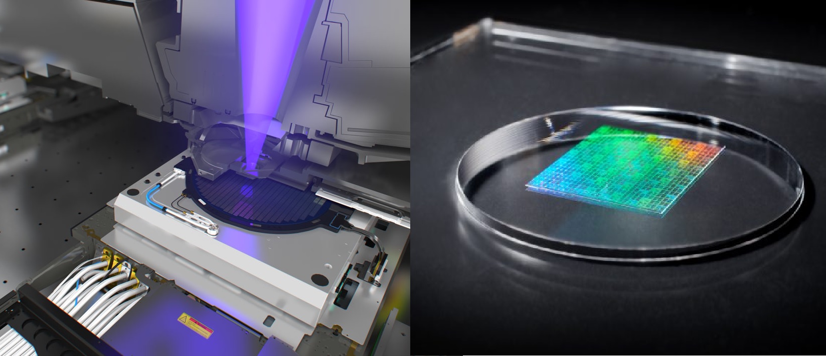
At the core of DNP’s update is a patterning template—the “stamp” in a stamping-style lithography flow. Instead of projecting light through complex optics (as in DUV/EUV), NIL physically presses a pre-formed pattern into a resist layer on the wafer, then cures it and transfers it through subsequent etch steps.
DNP says its new template achieves 10 nm circuit line width and is intended to support patterning for logic semiconductors aligned with the 1.4nm class, even though modern node labels no longer map cleanly to a single physical dimension on the chip.
To reach that resolution, DNP says it leveraged Self-Aligned Double Patterning (SADP)—a density-doubling technique widely used in advanced fabrication—applied here to the creation of the imprint template itself.
The Energy Claim That’s Turning Heads
DNP’s most attention-grabbing assertion is energy-related. The company says that, driven by its “energy-saving processing technology” using NIL, it can cut power consumption in the exposure process to approximately one-tenth compared with “currently available exposure processes,” including ArF immersion and EUV—depending on how the approach is deployed in a flow.
That claim speaks directly to a real industry pain point: EUV’s light source and tool infrastructure are widely viewed as power intensive, and EUV scanners are also famously large and costly, reinforcing why chipmakers obsess over reducing the number of EUV layers and rework steps in a leading-edge process.
Not A Full EUV Replacement — But A Strategic Alternative
DNP is careful about scope. It says the 10 nm NIL template could replace a portion of the EUV lithography process, including for customers that do not have EUV processing capacity but still want access to advanced patterning options.
Independent coverage has echoed the same framing: NIL is increasingly being pitched as a complementary patterning route for selected layers, not a wholesale swap for EUV across an entire 1.4nm-class logic flow.
This distinction matters because logic manufacturing at the leading edge is dominated by tight overlay and defect requirements across many layers. NIL’s contact-based approach can be unforgiving: particles, template wear, and alignment stability can all turn into yield killers if not controlled at scale. Those risks—overlay, defects, and template durability—are long-recognized challenges for nanoimprint as it moves from specialty applications toward mainstream logic ambitions.
Timeline: Evaluation In 2026, Production Targeted For 2027
DNP says it has begun evaluation work with semiconductor manufacturers and is aiming to start mass production in 2027, while expanding capacity to match demand.
Commercially, the company has put a number on its ambition: DNP is targeting ¥4 billion in NIL-related sales by FY2030.
The company also planned to show the new 10 nm template at SEMICON Japan 2025 (Dec. 17–19) at Tokyo Big Sight, signaling that it wants early ecosystem feedback and toolchain discussions to start immediately.
Why Japan’s Nanoimprint Push Is Gaining Momentum
DNP is not alone in pushing imprint back into the spotlight. Canon has been developing nanoimprint lithography tools for years and has already commercialized a 300mm NIL system that patterns by pressing a mask into resist “like a stamp,” explicitly emphasizing reduced power consumption and lower cost versus conventional optical exposure approaches.
Meanwhile, leading foundries are planning their 1.4nm-class eras on aggressive timelines—typically still EUV-heavy—while debating when, and whether, to transition to next-generation “High-NA” EUV tools. The backdrop creates an opening for technologies that can meaningfully reduce EUV tool count, EUV layer usage, or the overall exposure burden without forcing a full redesign of manufacturing lines.
The Remaining Challenges: Defects, Overlay, And Durability
For NIL to earn a place in advanced logic manufacturing, the industry’s questions are likely to be brutally practical.
First is defectivity control. NIL transfers patterns through physical contact; any contaminant can imprint directly into resist and propagate through etch, threatening yield. Second is overlay—the ability to align each layer to the one beneath it with nanometer-level accuracy across a full 300mm wafer. Third is template durability and repeatability: high-volume fabs cannot afford frequent template degradation, slow inspection cycles, or costly master replacements. These are exactly the issues that have historically kept NIL from taking over the most critical logic layers, even as the technique proved itself in other markets.
DNP’s 10 nm template achievement does not automatically solve those problems—but it does raise the stakes of the conversation. With evaluation programs underway and a 2027 manufacturing target, the next 12–24 months will likely determine whether NIL becomes a niche assist technology, a serious EUV load-reducer in select layers, or another promising approach that struggles under the realities of high-volume leading-edge production.
About the Author
Aditya Kumar:
Defense & Geopolitics Analyst
Aditya Kumar tracks military developments in South Asia, specializing in Indian missile technology and naval strategy.