India's Leap into Advanced Chip Design: Inauguration of 3nm Design Centres in Noida and Bengaluru
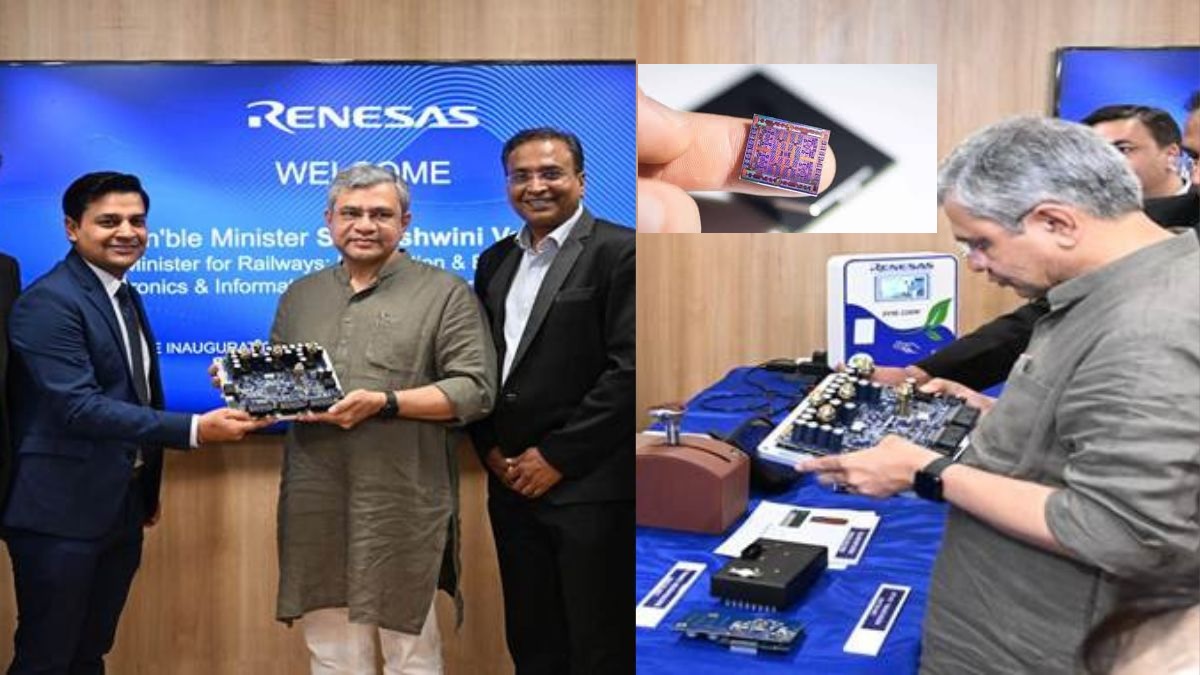
India has achieved a significant milestone in the semiconductor industry with the inauguration of its first 3-nanometer (3nm) chip design centres in Noida and Bengaluru. These state-of-the-art facilities, established by Renesas Electronics India Private Limited, were officially opened by Union Minister for Electronics & Information Technology, Railways, and Information & Broadcasting, Shri Ashwini Vaishnaw. This development marks India's entry into the advanced segment of chip design, positioning the country alongside global leaders in semiconductor innovation.
Advancing to 3nm Technology
The transition to 3nm chip design represents a significant technological advancement. Compared to previous generations like 7nm and 5nm, 3nm chips offer enhanced performance, reduced power consumption, and greater efficiency. These attributes are crucial for a wide range of applications, including smartphones, laptops, servers, medical devices, defense equipment, and automobiles. Minister Vaishnaw emphasized that this move sets a new standard in India's semiconductor capabilities.
Strengthening the Semiconductor Ecosystem
The Indian government is actively working to develop a comprehensive semiconductor ecosystem. This includes not only chip design but also fabrication, assembly, testing, marking, and packaging (ATMP), as well as the establishment of robust supply chains for equipment, chemicals, and gases. Global confidence in India's semiconductor vision is evident, with significant investments from companies like Applied Materials and Lam Research.
Empowering Talent and Innovation
To nurture a skilled workforce, the government has introduced a semiconductor learning kit aimed at enhancing practical hardware skills among engineering students. Over 270 academic institutions have already received advanced Electronic Design Automation (EDA) software tools under the India Semiconductor Mission. These institutions will now also receive hands-on hardware kits, integrating software and hardware learning to produce industry-ready engineers. This initiative is part of a broader strategy to invest in long-term talent development.
Renesas' Commitment to India
Renesas Electronics views India as a strategic cornerstone for its operations. The company is expanding its end-to-end semiconductor capabilities in the country, from architecture to testing. Through government-backed initiatives like the Chips to Startup (C2S) Program and the Design Linked Incentive (DLI) Scheme, Renesas supports over 250 academic institutions and numerous startups. The company's growing presence in India underscores its commitment to fostering innovation and contributing to the global semiconductor lifecycle.
A Vision for Self-Reliance
Minister Vaishnaw expressed gratitude to Prime Minister Shri Narendra Modi for prioritizing semiconductors as a strategic focus under the Aatmanirbhar Bharat vision. He highlighted that within just three years, India's semiconductor industry has evolved from a nascent stage to an emerging global hub. With the increasing demand for semiconductors across various sectors, this momentum is timely and positions India for sustainable growth in the industry.
The inauguration of the 3nm chip design centres in Noida and Bengaluru signifies a pivotal step in India's journey towards technological self-reliance and global competitiveness in the semiconductor sector.
✍️ This article is written by the team of The Defense News.